In this article:
- Introduction
- Intel Core Ultra Processors: Meteor Lake
- Intel Core Ultra H-Series
- Intel Core Ultra U-Series
- Summary
Introduction
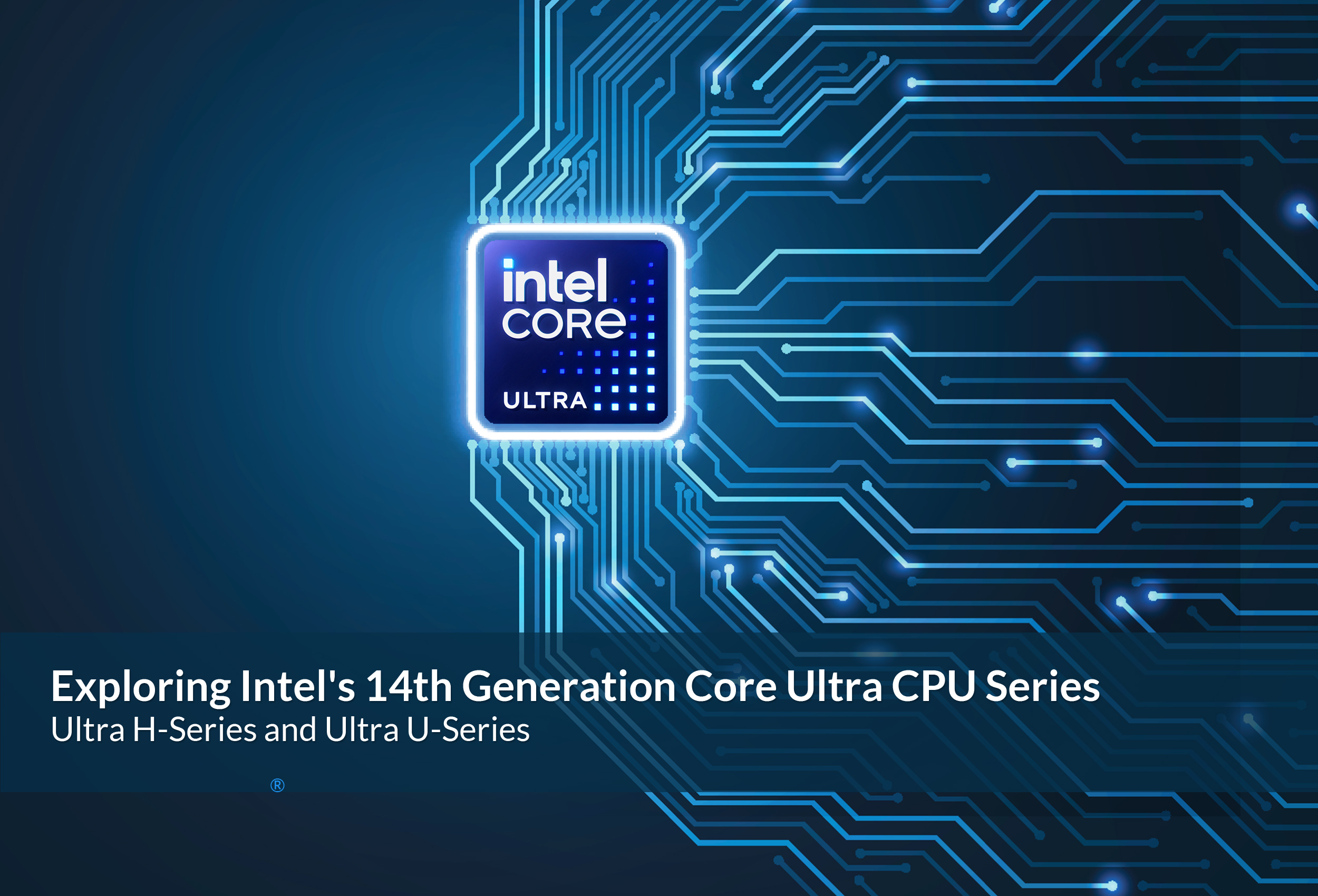
Towards the end of 2023, Intel unveiled its inaugural mobile processors hailing from the much-anticipated Meteor Lake platform. In this article we take an in-depth look at the Intel Core Ultra H-series and Core Ultra U-series.
The Ultra Core H series debuts with four distinct SKUs, featuring two Ultra 7 16-core (6P+8E+2LP) chips and two 14-core (4P+8E+2LP) Ultra 5 chips. Operating at a base TDP of 28 W, these processors boast a maximum turbo TDP of up to 115 W. Tailored for ultra-portable notebooks and similar compact devices, the Core Ultra-H series delivers heightened computing and graphics performance packaged within a sleek design.
Simultaneously, Intel has revealed the Intel Core Ultra U-series, comprising four SKUs with base/turbo TDPs of 15/57 W. This lineup includes two Core Ultra 7 and two Core Ultra 5 SKUs, each offering variations in P and E-core configurations, alongside Intel’s latest integrated Arc Xe graphics frequencies. Notably, all processors in the Core Ultra U-series sport 10 CPU cores, consist of two Performance cores and eight Efficiency cores, making them well-suited for low-powered and ultra-thin notebooks.
The debut of Intel’s tile-based Meteor Lake SoC signals the commencement of a new era of power-efficient and AI-centric chips on Intel 4 for the mobile market. This initiative aims to address the escalating demand for on-chip AI inferencing capabilities. Both the Intel Core Ultra H and U families integrate two innovative Low Power Island (LP-E) cores tailored for light workloads, along with two Neural Compute Engines housed within the Intel AI NPU, dedicated to handling generative AI inferencing tasks.
Intel Core Ultra Processors: Meteor Lake
In September 2023, Intel introduced its revolutionary chiplet-based Meteor SoC architecture during its annual Innovation event, reshaping the traditional monolithic processor into four distinct tiles. Leveraging their Foveros 3D packaging technology, Intel amalgamates various process nodes to craft its inaugural chiplet-based CPU.
The centrepiece of this architecture, the CPU tile, is meticulously crafted on Intel’s cutting-edge EUV-based Intel 4 node, heralded as the pinnacle of FAB technology, promising substantial enhancements in performance and energy efficiency over the longstanding Intel 7 process. Complementing the CPU tile are tiles dedicated to the integrated GPU, SoC, and I/O functions, amalgamating a blend of trailing-edge and external process nodes.
A succinct overview of the Meteor Lake SoC architecture reveals four interconnected tiles: compute, graphics, SoC, and I/O. Each tile hosts a myriad of innovations, including the Redwood Cove Performance (P) cores and Crestmont Efficiency (E) cores housed within the compute tile. Additionally, Intel introduces a specialised variant of the E-core, known as the Low Power Island or LP-E core, integrated into the SoC tile, specifically engineered to handle low-intensity workloads. Notably, due to the perpetual activity of the SoC tile, the LP-E core presents an exceptionally cost-effective energy solution compared to activating the CPU tile.
Meteor Lake represents a notable upgrade and a substantial architectural departure for Intel, transitioning from conventional monolithic designs to a chiplet-based methodology. Embracing Intel’s Foveros 3D packaging technology, this transition introduces 3D chip stacking, effectively surmounting the constraints associated with traditional 2D chip layouts. Following the trend observed in other transitions toward chiplet utilisation, this architectural paradigm emphasises disaggregation, power efficiency, and silicon flexibility, providing Intel with novel avenues for constructing CPUs from individual blocks.
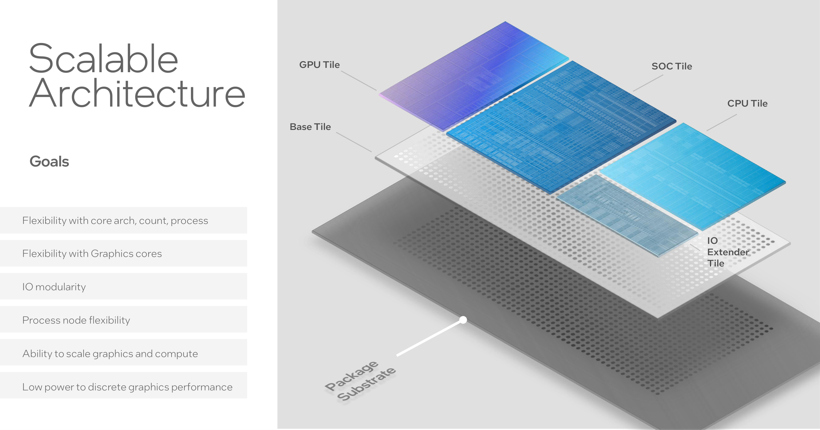
The modular design of the architecture enables scalable power management, allowing for optimisation where each tile operates autonomously, thereby enhancing both performance and energy efficiency. This disaggregated approach empowers Intel to leverage diverse silicon processes for individual tiles, thereby fostering flexibility and cost-effectiveness in manufacturing.
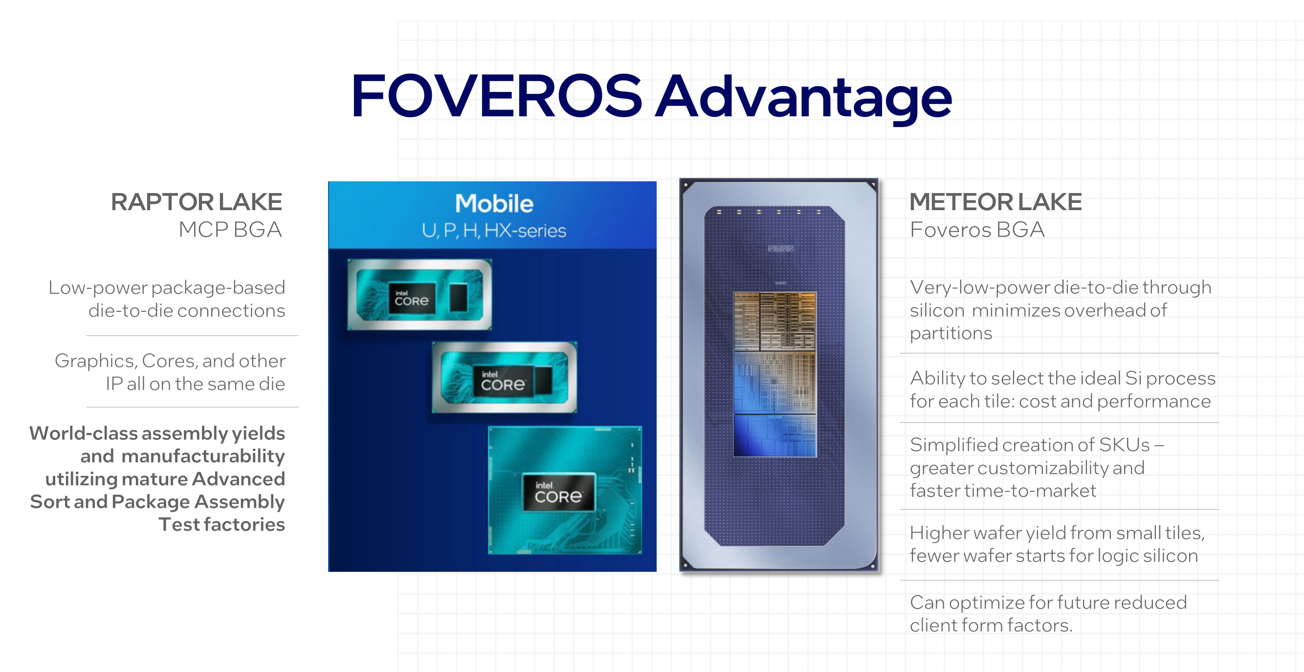
Departing from the Multi-Chip Packaging (MCP) utilised in previous Raptor Lake mobile chips, Meteor Lake adopts Foveros packaging alongside low-power, low-distance die-to-die interconnects. This shift permits more streamlined power utilisation and facilitates enhanced chip customisation, marking a significant advancement in chip architecture.
With four distinct yet highly functional tiles, Intel’s Meteor Lake is poised to revolutionise the customisation of their notebook SKUs in the future. This tile-based solution empowers Intel to integrate a diverse array of engines, blocks, and tiles into a single chip. Leveraging their Foveros packaging technology not only enables Intel to vary chip construction but also mitigates the risk associated with reliance on a single manufacturing process, providing a safeguard against issues with any particular fab or node.
Even in the current announcement of the Core Ultra U and H series chips, Intel demonstrates this versatility by employing different manufacturing processes for each tile. For instance, while the compute tile is constructed on Intel’s 4 node, the graphics tile featuring Arc Xe graphics utilises TSMC’s N5 node, with the SoC and I/O tiles built using TSMC’s N6 process. This strategic flexibility allows Intel to incorporate cutting-edge technologies from various process nodes, leveraging each node’s strengths (such as frequency or density) without necessitating the production and yield challenges associated with an entire chip on a leading-edge process.
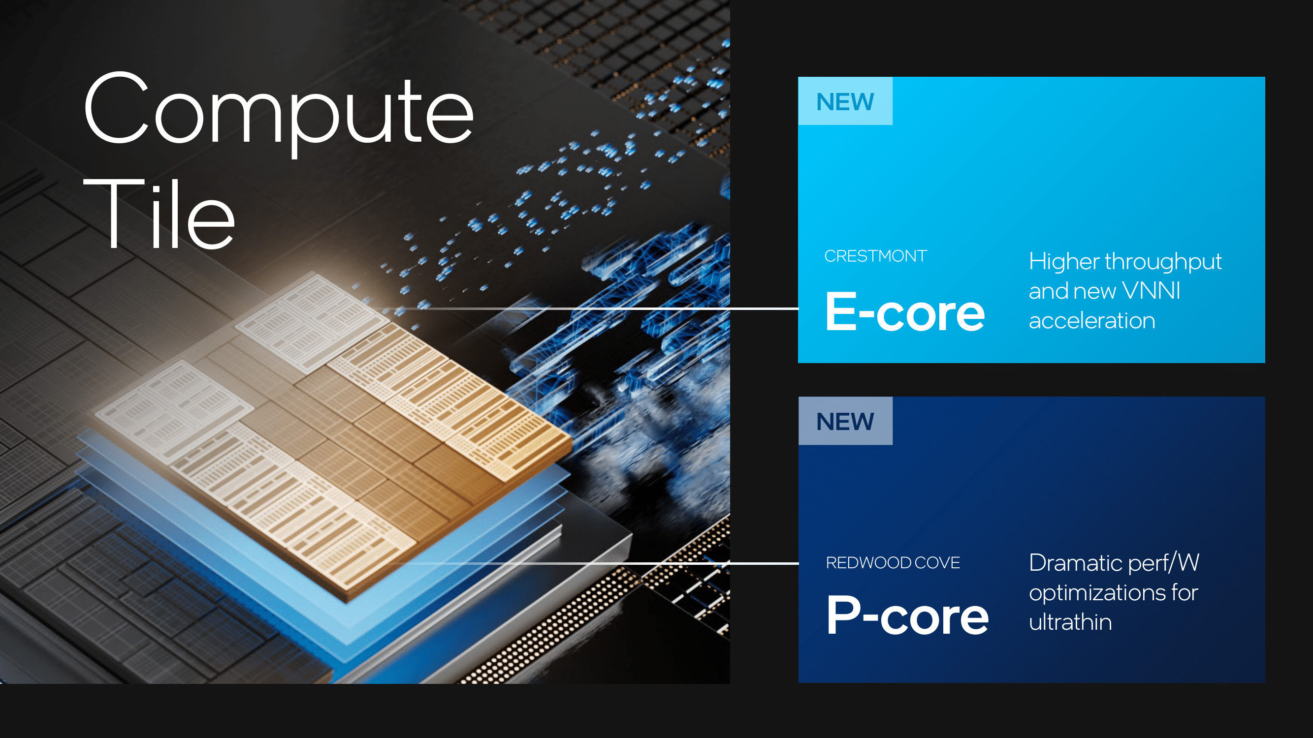
Examining the foundational architecture, the compute tile of the Ultra Core series within the initial release of Meteor Lake showcases Intel’s utilisation of two novel CPU architectures within a heterogeneous design. Constructed on the Intel 4 node, the Meteor Lake compute tile offers a 2x area scaling for the high-performance logic libraries compared to the preceding Intel 7 node. The latest Performance cores, dubbed Redwood Cove, introduce several enhancements over the previous Golden Cove P-core iteration, including superior per-watt performance efficiency, enhanced feedback facilitated by Intel Thread Director within Windows 11, increased bandwidth, and enhanced performance monitoring capabilities. These collective improvements are tailored to furnish comprehensive feedback to Thread Director, aiding in core performance optimisation and workload allocation.
However, notably absent from Intel’s disclosures is any mention of Redwood Cove’s IPC (Instructions Per Clock). Implicitly, this suggests that Redwood Cove’s IPC remains akin to, if not identical to, Golden Cove’s. Consequently, this implies that Intel may not achieve significant advancements in single-threaded performance in this generation, particularly in TDP-unconstrained scenarios. In fact, the peak P-core clock speeds for Core Ultra (Meteor Lake) chips are marginally lower than those of 13th Gen Core Mobile (Raptor Lake) chips – 5.1GHz versus 5.4GHz – suggesting a possibility that certain Core Ultra chips could fall behind in single-threaded CPU benchmarks compared to their 13th Gen Core counterparts.
Overall, while Intel is expected to realise tangible real-world performance gains owing to energy efficiency enhancements, the architectural shift to Redwood Cove appears more akin to a lateral move.
Conversely, Intel’s efficiency cores promise a substantial leap forward. The adoption of Crestmont cores for the efficiency cores is projected to yield IPC improvements over the 13th Gen Raptor Lake E-cores, alongside AI acceleration optimisations in Vector Neural Network Instructions (VNNI) and Instruction Set Architecture (ISA), along with enhanced feedback to Intel Thread Director. To bolster power efficiency, Intel integrates two new Low Power Island (LP-E) cores on each of the announced SKUs, housed within the SoC tile, effectively offloading light workloads onto these cores. The orchestration facilitated by Intel Thread Director within Windows 11 plays a pivotal role in ensuring optimal workload distribution across cores, thereby optimising performance and power efficiency levels.
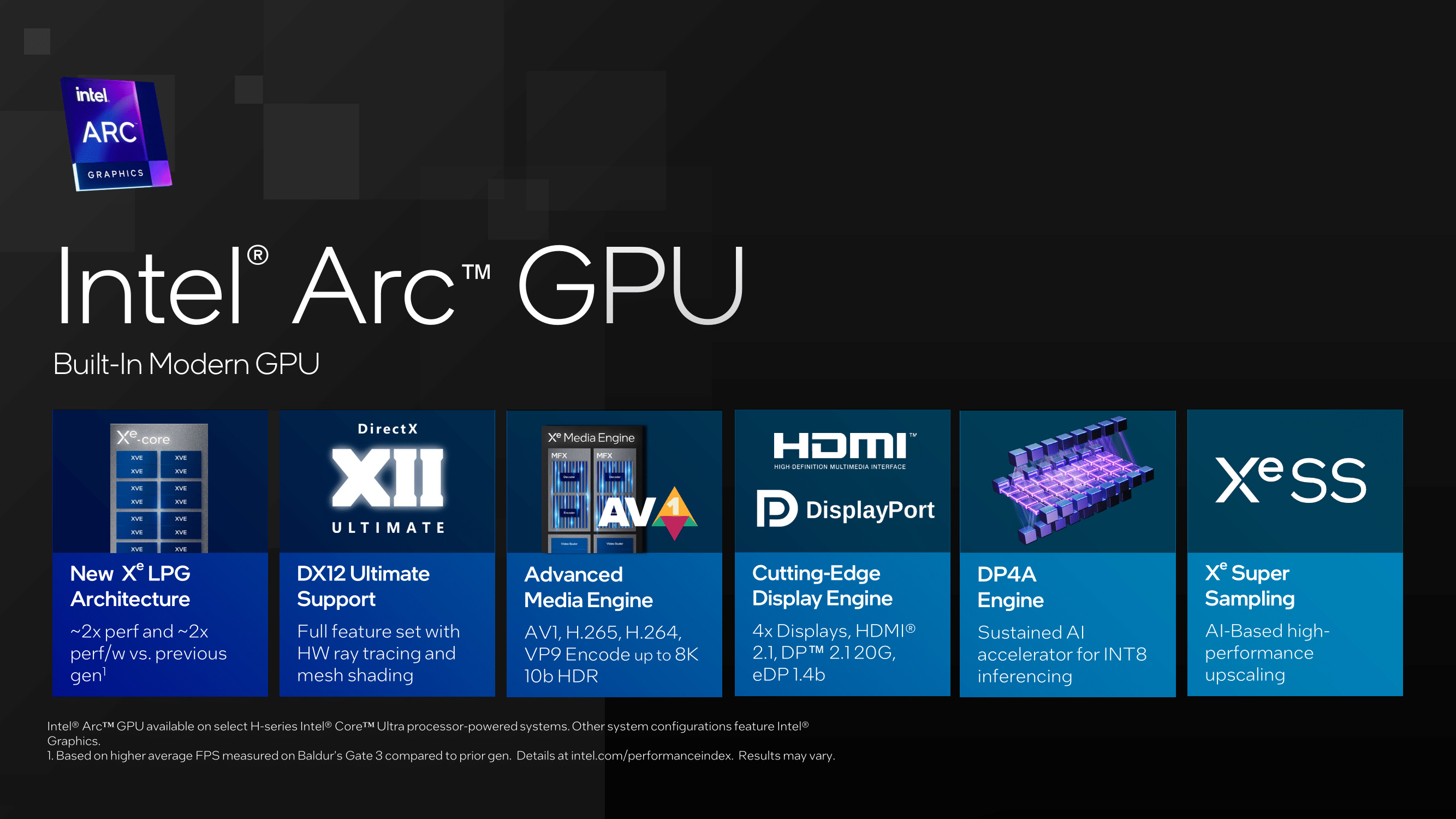
Another pivotal element within the diverse Meteor Lake SoC design is the enhancement to Intel’s Arc graphics architecture. Developed on TSMC’s N5 node, the selected graphics core is the Arc Xe-LPG core, stemming from Intel’s discrete Xe-HPG GPU architecture. Comprising 16 Vector Engines with a 256-bit bus width and 192 KB of shared L1 cache per core, the GPU tile exhibits remarkable capabilities. Each Vector Engine can execute 16 FP32 and 32 FP16 operations per clock cycle, accompanied by a shared FP64 execution port capable of 64 INT8 operations per clock.
Additionally, a dedicated FP64 unit, a novelty compared to Raptor Lake (13th Gen), enhances efficiency through pairs of vector engines operating in synchrony. Notably, this architecture excludes Intel’s matrix engines (XMX), limiting the GPU’s AI processing capabilities compared to desktop hardware, albeit still capable of executing AI tasks.
For Meteor Lake, Intel has chosen to separate the Xe Media Engine from the graphics tile and embed it within the SoC tile, fabricated on TSMC’s N6 node. This strategic move aims to enhance power efficiency by offloading encoding and decoding tasks from the GPU. The Xe Media Engine comprises two multi-format codecs (MFX), specifically designed for encoding and decoding operations.
Meteor Lake boasts extensive codec support, including AV1, HEVC, AVC, and VP9, with capabilities extending to decoding up to 8K60 HDR content. Furthermore, the Xe Media Engine is proficient in handling encoding tasks, supporting up to 8K 10-bit and HDR content.
Intel Core Ultra H-Series
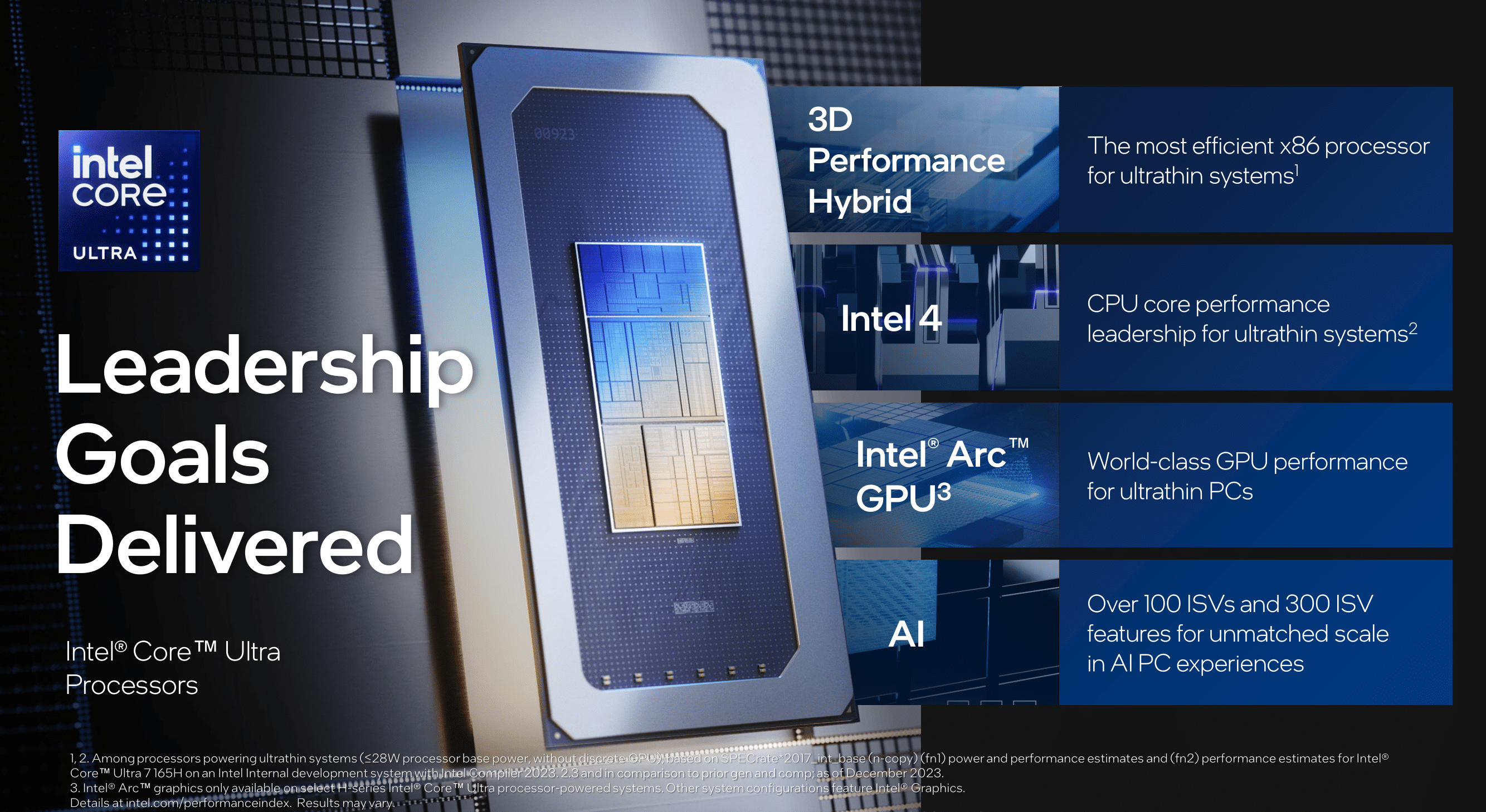
With the debut of Intel’s Core Ultra H and U-series, these chips mark the introduction of Intel’s new processor branding. Representing the most significant branding overhaul from Intel in the past 15 years, the Core Ultra 9, 7, and 5 series aim to categorise client chips into easily identifiable segments, with the Ultra designation reserved for premium offerings. A notable departure is the abandonment of the ‘i’ prefix, a hallmark of Intel’s processor identities for over a decade and a half, as seen in designations like Core i5.
Under the Core Ultra branding for the H-series, Intel is launching four SKUs spanning the Ultra 7 and Ultra 5 segments. However, the flagship Ultra 9 chips will remain absent for another quarter, with the Core Ultra 9185H not expected to debut until Q1 2024. It’s important to note the mixed messaging from Intel here.
Traditionally, U-series SKUs are tailored for ultrathin notebooks and ultraportables, yet Intel appears to suggest that the H-series could also find application in thinner notebooks. The validity of this claim remains to be seen, and clarity will emerge as OEMs and vendors unveil models featuring Meteor Lake.
Beginning with an analysis of the available chip specifications, the Core Ultra 7 165H and Core Ultra 7 155H are both 16C/22T processors. Featuring six performance (P) cores and eight efficiency (E) cores, along with two LP-E cores on the SoC tile, these chips boast a total of 16 CPU cores capable of executing up to 22 threads simultaneously.
The Core Ultra 7 165H boasts a P-core turbo frequency of up to 5.0 GHz and an E-core turbo frequency of up to 3.8 GHz. Additionally, it integrates 8 Intel Arc Xe cores for graphics, clocking up to 2.3 GHz, and includes 24 MB of Intel Smart L3 cache.
Slightly slower, the Intel Core Ultra 7 155H features a P-core turbo of 5.0 GHz and an integrated graphics frequency of 2.25 GHz. Its Crestmont E-cores can reach a maximum of 3.8 GHz, and it also includes 24 MB of L3 cache. The only distinction between the two Core Ultra 7 SKUs lies in a 100 MHz decrease in P-core turbo frequency and a slight 50 MHz reduction in graphics clock speed.
Both chips operate within a broad TDP range. The base TDP for the Ultra 7 (and Ultra 5) H-series parts is set at 28 Watts, with turbo modes ranging from 64 Watts to 115 Watts for the fastest devices. Considering these are mobile parts, it’s important to note that device vendors have significant flexibility in adjusting TDP limits to align with power and cooling constraints.
It’s noteworthy that Intel primarily compares many of the Core Ultra H-series chips against the previous 13th Gen Raptor Lake-Based P-SKUs (28/64 W) in terms of performance, rather than the 13th Gen H-series parts. This generation sees a reduction in the base TDP for the H-series, from 45 W down to 28 W. Intel appears to consolidate the P and H series (which were already utilising the same silicon and packages) into a single line, the H-series, for the inaugural Core Ultra generation.
Now delving into the Core Ultra 5 series SKUs, akin to the Core Ultra 7 H-series, there are subtle differentiations in specifications. The swifter of the duo, albeit boasting a 100 MHz higher P-core turbo, is the Core Ultra 5 135H, presenting a 14C/18T configuration with 4 P-cores and 8 E-cores constituting the compute tile. The Core Ultra 5 135H flaunts a 4.6 GHz P-Core turbo and a 3.6 GHz E-core turbo. However, it features a slightly lower specification Intel Arc graphics tile housing 7 Xe graphics cores, capable of reaching up to 2.2 GHz.
Conversely, the Core Ultra 5 125H showcases a 4.5 GHz P-Core turbo, matching the 3.6 GHz E-core turbo of the 5 135H, and shares the same Arc integrated graphics clocked at 2.2 GHz. Both the Intel Core Ultra 5 135H and Core Ultra 5 125H exhibit a base TDP of 28 W, accompanied by Intel’s provision of a 64 or 115 W turbo TDP specification.
The final entry among the announced Intel Core Ultra H-series SKUs, slated for release in Q1 2024, is the Core Ultra 9 185H. Despite coincidentally boasting the highest specifications, the Core Ultra 9185H aligns with the 6P+8E+2LP/22T architecture akin to the two Core Ultra 7 chips unveiled earlier.
Sporting P-Core turbo clock speeds of up to 5.1 GHz and an E-Core turbo frequency of 3.8 GHz, it features the same Arc-based 8 Xe cores within the graphics tile, clocked at up to 2350 MHz. Diverging from the other Core Ultra H-series processors, the Core Ultra 9185H bears a higher 45 W base TDP, alongside a maximum 115 W TDP at turbo clock speeds.
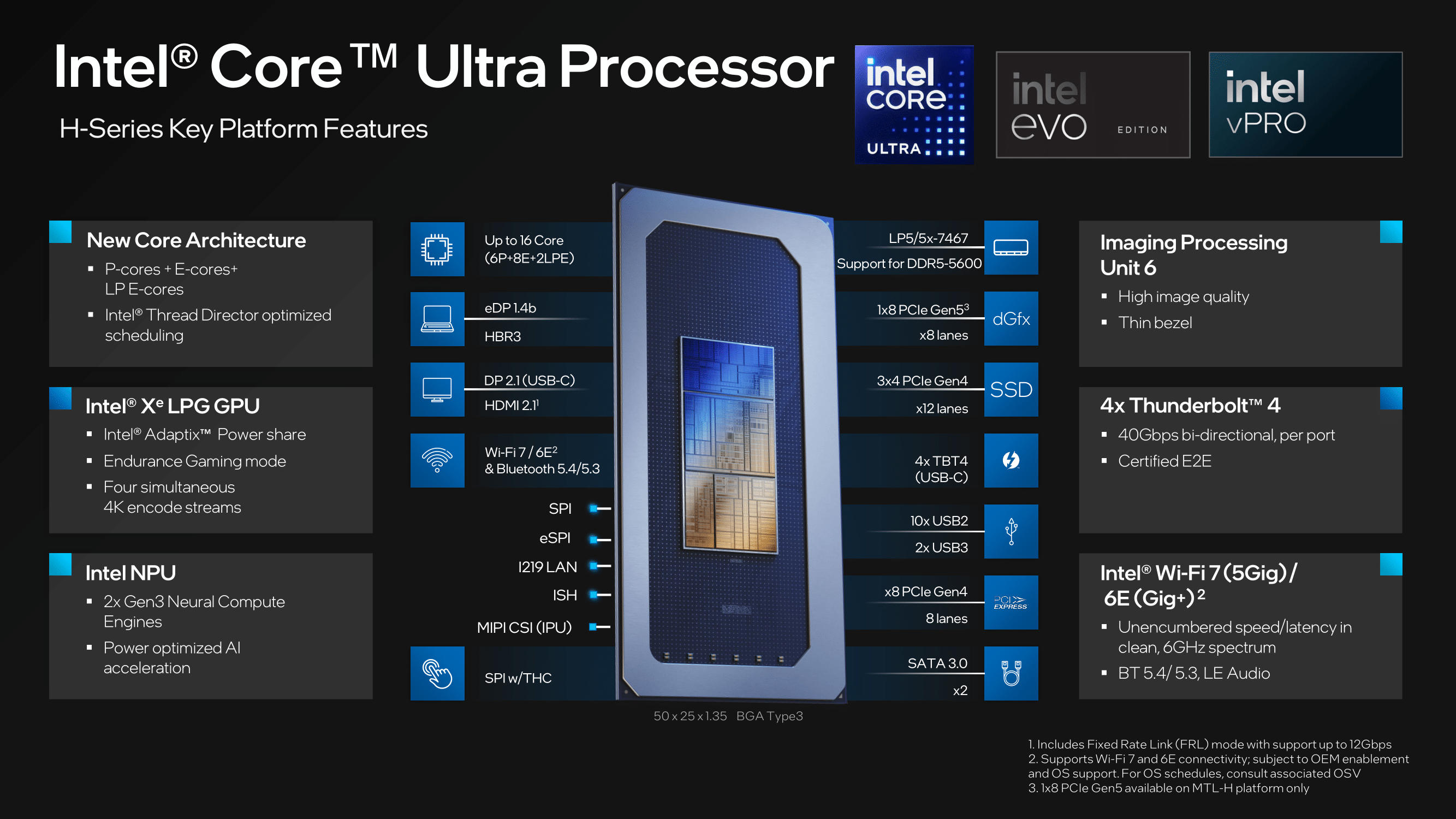
All Intel Core Ultra H series SKUs feature the inclusion of 2 Low Power Island (LP-E) cores directly integrated into the SoC tile. These cores are strategically designed to enhance power efficiency by assigning low-intensity workloads to the most efficient of the three available core types. Additionally, the SoC tile houses two Neural Compute Engines, Intel’s implementation of an NPU optimised for generative AI workloads.
In terms of memory support, the Core Ultra H-series platform accommodates both DDR5 and LPDDR5(X). Currently validated against DDR5-5600 and LPDDR5X-7467, these memory modules are connected via a 128-bit memory bus.
For internal I/O capabilities, Intel offers a blend of PCIe 5.0 and PCIe 4.0 lanes on the Core Ultra H-series platform. OEMs have access to a single PCIe 5.0 x8 link for integrating discrete graphics, alongside 12 PCIe 4.0 lanes dedicated to driving storage, supporting up to three PCIe 4.0 x4 M.2 SSDs. An additional 8 PCIe 4.0 lanes cater to general I/O requirements. For systems requiring additional storage options, particularly SATA III drives, there are two available SATA III ports on the chip.
On the external I/O front, the Core Ultra H-series platform provides support for 4x Thunderbolt 4 (USB4) ports, along with 2x USB 3 and 10x USB 2 ports. The integrated GPU can drive DisplayPort 2.1 video output via the Type-C ports, and the platform supports a dedicated HDMI 2.1 port if desired by OEMs.
Regarding wireless connectivity, the Meteor Lake platform natively supports Wi-Fi 6E, facilitated by the latest generation of Intel’s CNVio technology. This integration incorporates a Wi-Fi MAC into the host chipset (SoC), while the PHY remains a separate module. This design minimises costs for OEMs and reduces overall footprint.
While Intel lists Wi-Fi 7 support for Meteor Lake, it’s worth noting that this is entirely discrete. The Meteor Lake platform itself does not include native Wi-Fi 7 hardware. OEMs interested in integrating Wi-Fi 7 would need to include a standalone adapter, such as Intel’s BE200. Consequently, Wi-Fi 7 support is expected to be primarily limited to premium notebooks, where OEMs can justify the higher cost of a discrete adapter and accommodate its physical placement.
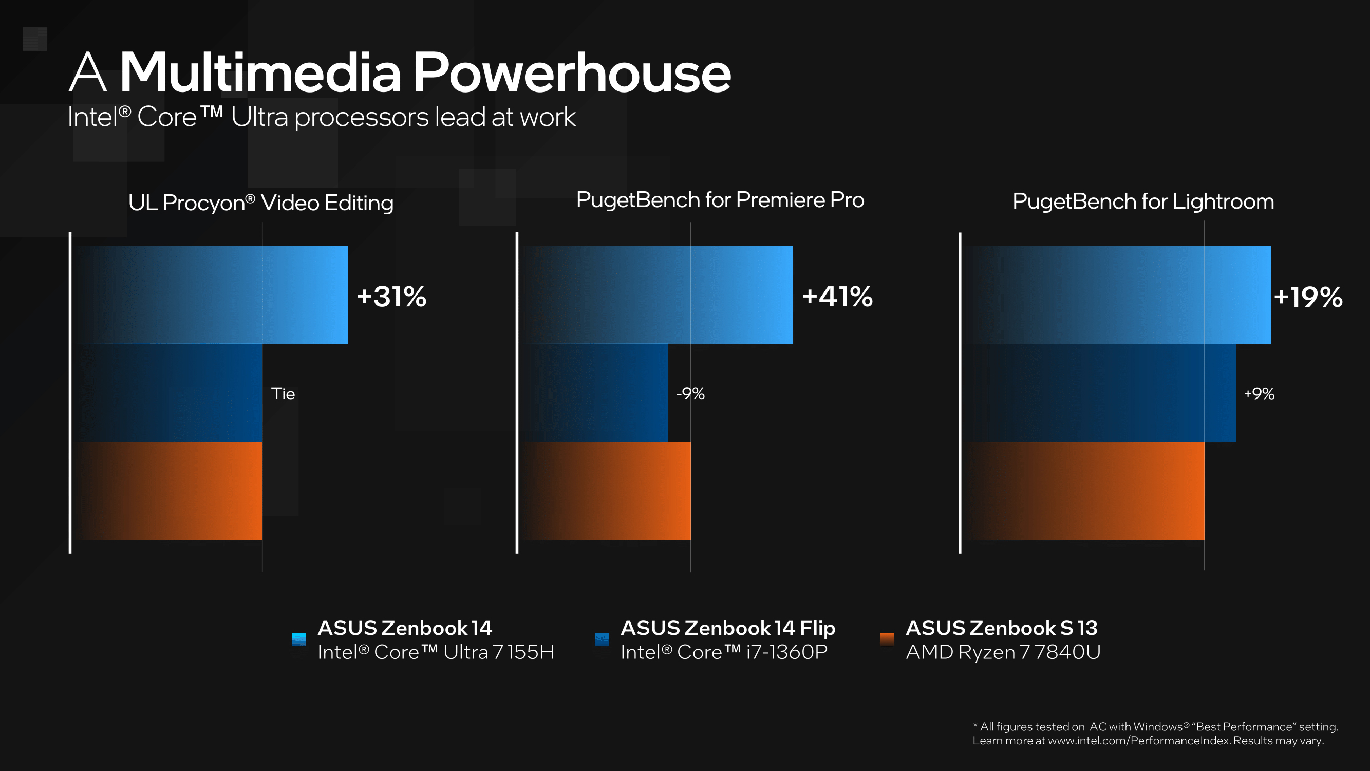
Examining the performance metrics presented in Intel’s Core Ultra series slide deck, notable figures emerge. Intel asserts a substantial performance improvement of up to 31% within UL Procyon’s video editing benchmark. Moreover, Intel claims an even more significant gain of 41% compared to the AMD Ryzen 7 7840U processor in PugetBench for Premiere Pro. In another benchmark scenario using PugetBench for Lightroom, Intel touts the Core Ultra 7 115H as 19% faster.
While it’s customary to approach vendor and manufacturer’s in-house performance figures with cautious scrutiny, these metrics nonetheless provide insights into the anticipated performance of new products.
Regarding GPU performance, Intel is conducted a comparative analysis between the latest Arc Xe-LPG integrated graphics on the Core Ultra 7 165H and the previous generation Core i7-1370P.
While Intel is evidently placing considerable emphasis on the Arc-based integrated graphics for Meteor Lake’s performance prowess, the forthcoming months will provide valuable insights into how this performance compares against discrete options.
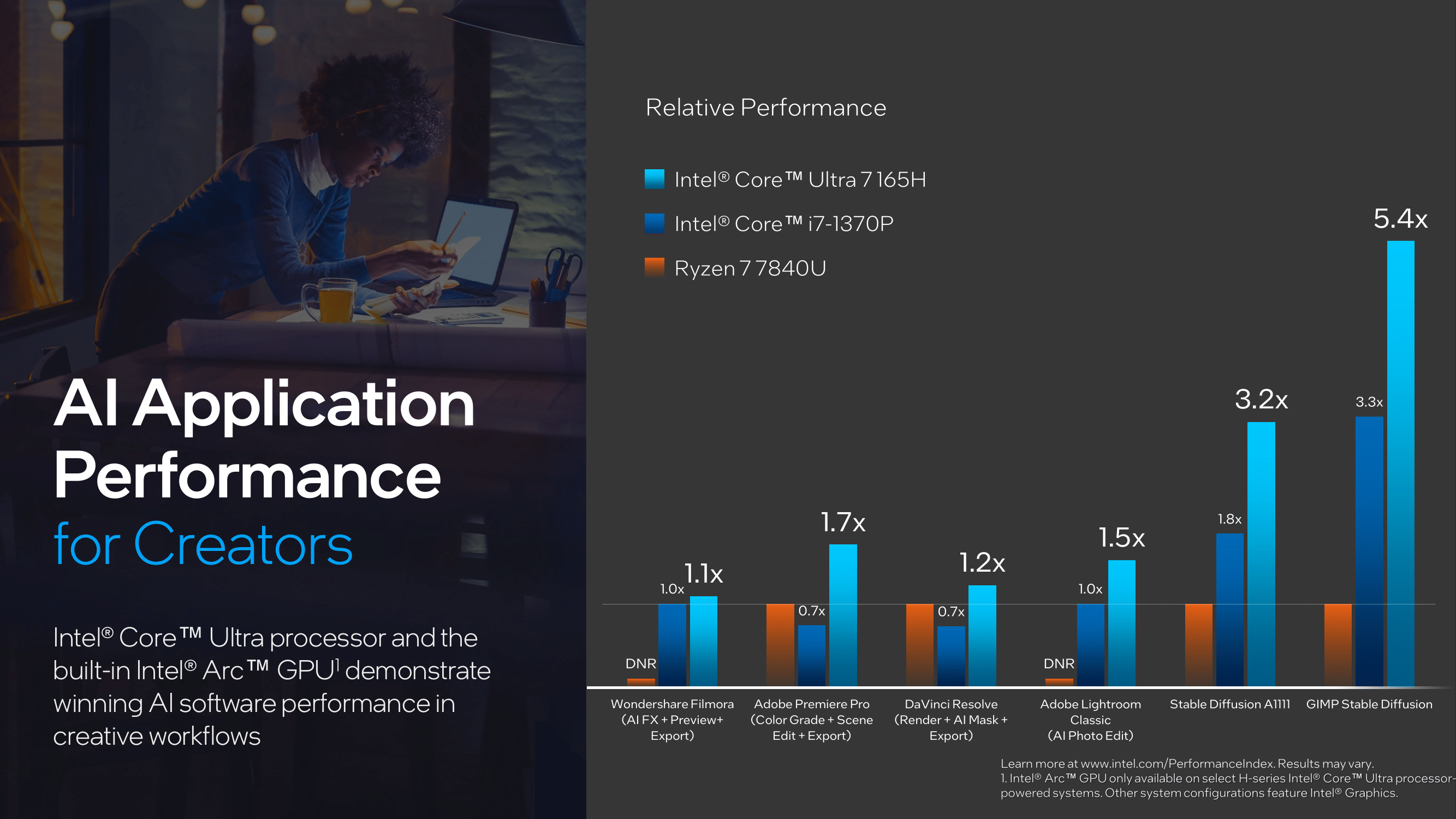
In the realm of AI performance, Intel is striving to demonstrate their advantage over the competition. They assert that there is up to a 5.4X performance improvement in GIMP Stable Diffusion solely through the enhanced capabilities of the Arc Xe-LPG graphics cores, compared to the previous Core i7-1370P and AMD Ryzen 7 7840U processor. Even in applications leveraging generative AI like Adobe Lightroom, Intel claims up to 1.5X the performance of the Ryzen 7 7840U.
However, it’s prudent to approach vendor and OEM-supplied performance figures with caution. While the performance gains showcased by Intel for the Core Ultra H series seem impressive on paper, real-world experiences and benchmarks may vary.
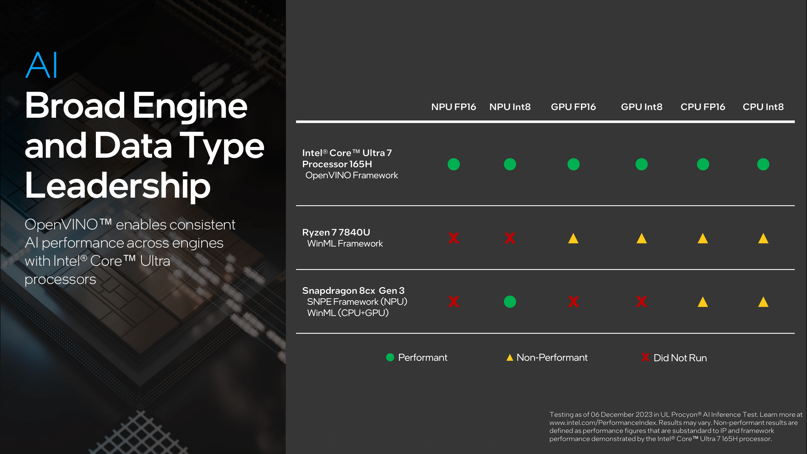
Intel’s Meteor Lake SoC embodies a comprehensive and multi-faceted approach to AI inferencing, leveraging generative AI capabilities across the compute, graphics, and NPU engine blocks. Intel emphasises the presence of three fully functional AI engines within Meteor Lake, highlighting the Arc Xe-LPG graphics for high-throughput AI acceleration in content creation tasks. Conversely, the NPU, complemented by its two Neural Compute Engines, is tailored to offload sustained AI workloads, thereby enhancing power efficiency. The Compute tile, alongside the combination of Redwood Cove (P) and Crestmont (E) cores, is engineered to handle AI tasks with lower latency, ensuring precision.
With the PC CPU ecosystem now vigorously integrating improved AI and neural network capabilities into their designs, a competitive landscape is emerging, with vendors vying to showcase their NPU capabilities and performance. As Intel enters this domain with its latest launch, the company underscores its support for a wide array of numerical formats. Moreover, Intel capitalises on its established OpenVINO framework to harness the combined AI capabilities of its CPU, GPU, and NPU hardware.
Intel’s in-house testing, as depicted in the provided chart running the UL Procyon AI inference benchmark, presents a somewhat complex comparison due to the benchmark’s support for various vendor-specific backends. Consequently, real-world experiences and performance may vary, and users should interpret these benchmarks with due consideration.
Intel Core Ultra U-Series
Transitioning to the new Intel Core Ultra U-series processors, Intel presents four SKUs currently available, with an additional two slated for release in Q1 2024.
First in line is the Intel Core Ultra 7 165U, featuring a 2P+8E+2LP/14T configuration. This chip boasts a P-core turbo frequency of up to 4.9 GHz and an E-core turbo frequency of 3.8 GHz. With 4 Xe integrated graphics cores clocked at 2.0 GHz, the Core Ultra 7 165U delivers balanced performance.
In comparison, the Core Ultra 7 155U shares similar specifications but operates slightly slower. With a P-core turbo frequency of 4.8 GHz (100 MHz lower) and integrated graphics cores clocked at 1.95 GHz (50 MHz lower), the Core Ultra 7 155U offers a marginally reduced performance level.
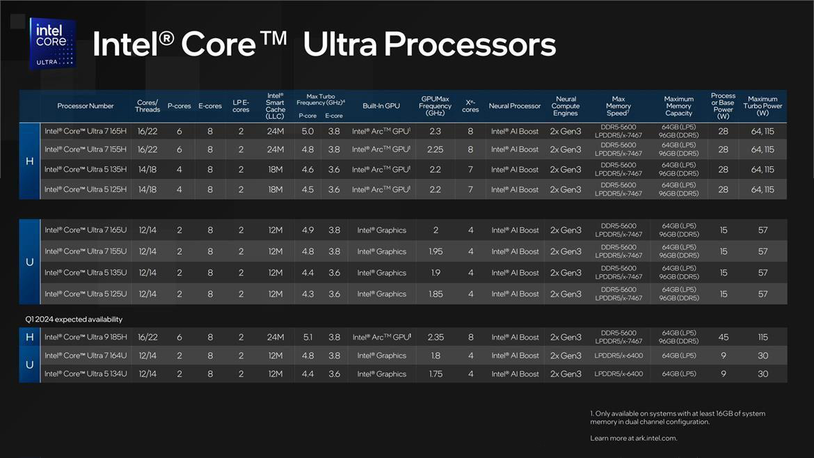
The Intel Core Ultra 5 (U) series encompasses three SKUs, with two available currently and one, the Core Ultra 5 134U, slated for launch in Q1 2024. Beginning with the Core Ultra 5 135U, it features a CPU core configuration of 2P+8E+2LP/14T, boasting a P-core turbo frequency of up to 4.4 GHz and an E-core turbo frequency of up to 3.6 GHz. Integrated with 4 Arc Xe graphics cores clocked at 1.9 GHz, and equipped with 12 MB of L3 cache, this chip offers robust performance. Similarly, the Core Ultra 5 125U shares the same core configuration but operates slightly slower, with a P-core turbo frequency of 4.3 GHz and integrated graphics cores clocked at 1.85 GHz.
All Core Ultra U-series processors announced today feature a 2P+8E configured compute tile, along with 4 Xe Arc integrated graphics cores, 12 MB of L3 cache, and a base TDP of 15 W and a turbo TDP of 57 W. Like their H-series counterparts, the U-series chips also integrate 2 Low Power Island LP-E cores within the SoC tile, alongside 2 Neural Compute Engine cores for AI inferencing and generative AI workloads.
While not explicitly depicted in Intel’s diagrams, the U-series chips offer similar internal and external I/O capabilities as the H-series chips, albeit with a focus on accommodating discrete graphics. They provide 12 PCIe 4.0 lanes for storage and another 8 PCIe 4.0 lanes for general I/O, along with support for 4x Thunderbolt 4 (USB4) ports, 2x USB 3, and 10x USB 2 ports.
However, the two Core Ultra U-series chips set for launch in Q1 2024 exhibit some differences. Notably, they feature a 9 W base TDP with a turbo TDP of 30 W, significantly lower than their counterparts. The Core Ultra 7 164U and the Core Ultra 5 134U maintain the same turbo clock speeds as the top series counterparts but offer lower Arc graphics frequencies, at 1.8 GHz and 1.75 GHz, respectively. These chips do not support DDR5 memory and are limited to LPDDR5(X) memory speeds up to 6400 MT/sec, tailored for ultra-low-power configurations.
Primarily designed for the thinnest and lightest notebooks and other small/slim devices, these chips prioritize low-TDP processors to align with cooling abilities and battery capacities. They are anticipated to utilise Intel’s Type4 chip packaging, ensuring optimal space utilisation in compact designs.
Summary
In summary, Intel’s unveiling of the Meteor Lake platform marks a significant shift towards chiplet-based architectures, demonstrating a commitment to innovation and versatility in their processor lineup. The Meteor Lake SoC introduces a modular design with interconnected tiles, offering enhanced power management and flexibility in manufacturing processes. With the Core Ultra H and U series, Intel introduces a new processor branding strategy, emphasising performance and customisation across a range of SKUs.
The Core Ultra H series boasts impressive specifications, delivering high-performance computing and graphics capabilities within ultra-portable notebooks. Meanwhile, the Core Ultra U series targets lower-powered and ultra-thin notebooks, prioritising energy efficiency without compromising on performance. Both series integrate advanced AI capabilities, leveraging a combination of CPU, GPU, and NPU engines to handle diverse workloads efficiently.
Intel’s emphasis on AI performance, GPU acceleration, and memory support underscores their commitment to meeting the evolving demands of modern computing. The integration of Low Power Islands LP-E cores, Neural Compute Engines, and advanced memory technologies further enhances the efficiency and versatility of Intel’s processors.
While Intel’s performance claims are notable, real-world experiences may vary, and users should interpret benchmarks with caution. However, the strides made in AI inferencing, GPU acceleration, and power efficiency signal promising advancements in Intel’s processor lineup.
Overall, the Meteor Lake platform represents a bold step forward for Intel, ushering in a new era of performance, efficiency, and customisation in mobile computing. With its chiplet-based architecture, modular design, and advanced AI capabilities, Intel is poised to meet the diverse needs of consumers and propel innovation in the mobile computing landscape.