Computer designers have been immensely focused upon size for many years now and it’s only in recent times that significant advancements have been made. In the industrial and embedded worlds, efficiency is critical; a key factor in achieving this is utilizing the capacity of your space to its maximum. Even more so when considering cloud integration, upgrading hardware or integrating a completely new system. The theory of Moore’s Law has for long stood rigid and true. It is however soon to be redundant.
![]()
Originally coined as a way to explain the ongoing improvements in transistor scaling after Intel co-founder Gordon Moore observed that the number of transistors per square inch had doubled every year since their invention- that was in 1965. Since then it has been redefined and extended to include long-term trends in semi-conductor performance and new chip features. The International Technology Roadmap for Semiconductors (ITRS) recently released an extensive update on the future of semiconductor technologies and it details that conventional 2D transistor scaling will likely end by 2021 to be replaced by new and different types of integration.
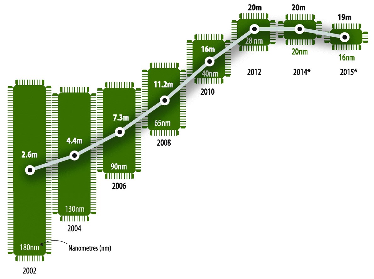
Moore’s Law has been revised numerous times as it continues to evolve with times. Recent times have seen attentions turn from 2D interconnecting of chips which have large sillicon footprints to the more costly but condensed system-on-chip (SoC) solution which thanks to their reduced size and increased performance have enabled smartphones to become such enveloping (but expensive) instruments with their wireless, touchscreen, cameras and vast storage features all thanks to a high speed SoC operating well above 1GHz.
What is an SoC?
An System-on-Chip is an integrated circuit that collates all components of a computer or other electronic device into one chip. This Chip can contain digital, analog, mixed-signal, and often radio-frequency functions—all on a single, low consumption chip.

The next generation of chipsets however are likely to begin their integration sometime between 2021 and 2024 and instead utilize 3D stacking. This not only reduces the overall footprint and hence, system size but also produces shorter interconnects for higher speed processing. This tally’s to become a comprehensive advancement when compared with SoC formats, SoC’s see a 15% reduction in size, 30% power/ signal improvements, with a 5% cost increase. 3D stacking however takes the progression of the SoC from the original 2D interconnect to another level. When they become a tangible possession, expect 35% reduction in size, 40% power/ signal improvements and a staggering 45% cost reduction. The shift from 2D to 3D structures will be a simple transition for some and much more complex for others. One of the major challenges is that in stacking memory transistors on top of logic transistors, one or both layers could melt due to the heat trapped between. This however is one of the stumbling blocks manufacturers will overcome with the use of specialist materials such as silicon-germanium.
A recent ITRS report is pretty clear, for significant CPU performance improvements, new computing architectures are required, improved memory performance in general or improved multi-threading are key, not clock speed. This as well as the old structures, leaves Moore’s Law behind. The report goes further to say that by 2029 they expect 25 application processors, 303 GPU cores, with a max single-component frequency of 4.7GHz.
The market demands low power over strict clock advances, especially with limited availability of current precious materials for higher clock speeds. However, even when the first 3D chips become integrated, they will be in the heart of IoT developments, not in your laptop or PC. This consistent desire for progression is one that is already present by enterprises and developers, and more so, readily available, we have a superb range of high performance SoC computers, with tiny footprints to maximize your space, installation and efficiency.
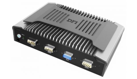
Our latest products from DFI are a fantastic example of flawless, compact design, built for computing excellence in the embedded industry with the very exciting high performance EC70A-SU and deeply embedded EC700-BT. See here for more information.
About Assured Systems
Assured Systems is a leading technology company offering high quality and innovative applied computing solutions to the embedded, industrial, and digital-out-of-home markets across the world. Headquartered in Stone, England and with offices in North America, our reach is truly global.